Scanning Electron Microscopes
Scanning Electron Microscopes
Two SEMs reside within ARES, a JEOL 7600F and a JEOL 7900F. These instruments provide
imaging and chemical analysis of meteorites, lunar samples, IDPs (interplanetary dust
particles), terrestrial materials, and experimental samples. Two types of electron
images are obtainable via our systems - secondary electron images (SEI) that show
topographic features (sample morphology) - and backscattered electron images (BEI)
that show compositional features. The SEMs are also used to examine samples from
space-exposed hardware surfaces that have been hit by high-velocity impactors,
where we endeavor to identify the nature of the impactor (micrometeoroid or orbital
debris) based on the chemical composition of condensates or residues from the
impacting particle.
Both of the SEMs (7600F and 7900F) produce ultra high-resolution electron images
using a thermal field emission electron gun. This type of gun is a significant
advancement over earlier types of W-filament based SEMs because of the remarkably
fine (~1–2 nm) electron beam delivered to the sample surface. The tightly focused
beam enables us to record electron images with 2–3 nm spatial resolution. Both the
7600F and 7900F SEMs are equipped with two different SEI detectors and two BEI
detectors. For both detector types, one is in-lens and one is in the sample chamber.
The in-lens detectors enable our researchers to position samples very close to the
bottom of the electron column, which permits the acquisition of images with a
low-energy beam. The advantage of a low-energy beam is that very near-surface features
are emphasized.
Both SEMs are equipped with 170 mm2 SDD type x-ray detector systems that are a
significant advance over earlier Si(Li) detectors in that they can acquire and
process >100,000 x-ray counts per second. This high-count rate allows for the
production of high-quality x-ray maps in reasonable times and enables rapid
chemical mapping of thin sections and epoxy impregnated mounts of various planetary
materials.
The 7900F is also equipped with a state-of-the-art crystal metal oxide semiconductor
(CMOS) based electron backscatter diffraction (EBSD) detector that enables pattern
acquisition speeds up to 3000 hertz, orders of magnitude faster than pervious CCD
based versions. Electron backscatter diffraction patterns (EBSPs) give absolute
crystallographic orientation data. EBSPs can be collected along rastered maps at
step size down to 50 nm, which can be used to characterize intracrystalline
misorientations and quantify plastic strain within grains. This technique is a
novel way of studying deformation and recrystallization processes in the solar
system such as shock metamorphism. Alternatively, focused ion beam thin foils can
be analyzed in transmission mode to enable fine resolution (~5 nm) microstructural
imaging, which can be used to guide future TEM analyses.
The Oxford Electron Backscatter Diffraction detector (EBSD) can collect high resolution
kikuchi patterns at ultra-fast speeds (3000 patterns per second). This technique can be
used for structural identification of mineral phases, quantification of intracrystalline
plastic strain within individual grains, and determination of deformation mechanisms.
Coupling EBSD with other spectra techniques (EDS, WDS, in situ isotopic analyses)
is being used to understand the way the building blocks of solar system have been reworked
throughout its history.’
The 7600F is also equipped with a SDD type x-ray detector system. This type of detector
is a significant advance over earlier Si(Li) detectors in that it can acquire and process
>100,000 X-ray counts per second. This high count rate permits us to produce high quality
X-ray maps of planetary samples in reasonable times. In the example shown here to the left,
an X-ray map of a portion of a chondritic meteorite, Mg is red, Ca is green, and S is blue.
Laboratory Leads
|
Lindsay Keller
NASA 281-483-6090 |
Loan Le
Jacobs JETS II 281-483-6186 |
Timmons Erickson
Jacobs JETS II 281-792-8609 |
Laboratory Leads
|
Lindsay Keller
NASA 281-483-6090 | |
|
Loan Le
Jacobs JETS II 281-483-6186 |
Timmons Erickson
Jacobs JETS II 281-792-8609 |
Electron Beam Laboratory Suite
The Electron Beam Laboratory Suite includes two scanning electron microscopes (SEM),
two transmission electron microscopes (TEM), two electron microprobes, one dual-beam
focused ion beam (FIB) instrument, one NanoSIMS 50L, and a one-of-a-kind laser microprobe.
These workhorse instruments are used to characterize all types of materials studied
within ARES, and virtually every research group makes frequent use of one or more
of these instruments while conducting research in support of the ARES mission.
Electron Beam Laboratories
Electron Beam Laboratories
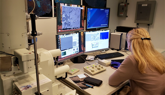 Inside the Scanning Electron Microprobe Laboratory:
Planetary scientist Kathie Thomas-Keprta collects EDX spectra of the Mars meteorite ALH84001.
Inside the Scanning Electron Microprobe Laboratory:
Planetary scientist Kathie Thomas-Keprta collects EDX spectra of the Mars meteorite ALH84001.